
- English
- Español
- Português
- русский
- Français
- 日本語
- Deutsch
- tiếng Việt
- Italiano
- Nederlands
- ภาษาไทย
- Polski
- 한국어
- Svenska
- magyar
- Malay
- বাংলা ভাষার
- Dansk
- Suomi
- हिन्दी
- Pilipino
- Türkçe
- Gaeilge
- العربية
- Indonesia
- Norsk
- تمل
- český
- ελληνικά
- український
- Javanese
- فارسی
- தமிழ்
- తెలుగు
- नेपाली
- Burmese
- български
- ລາວ
- Latine
- Қазақша
- Euskal
- Azərbaycan
- Slovenský jazyk
- Македонски
- Lietuvos
- Eesti Keel
- Română
- Slovenski
- मराठी
- Srpski језик
China Cvd sic Pengilang, Pembekal, Kilang
CVD SiC is a vacuum deposition process used to produce high-purity solid materials. This process is often used in semiconductor manufacturing to form thin films on wafer surfaces. During the chemical vapor deposition (CVD) process for producing silicon carbide (SiC), a substrate is exposed to one or more volatile precursors, which chemically react on the substrate surface to form the desired SiC deposit. Among the various methods for producing SiC, CVD produces products with high uniformity and purity, and offers strong process controllability.
Simply put, CVD SiC refers to SiC produced via the chemical vapor deposition (CVD) process. In this process, gaseous precursors, typically containing silicon and carbon, react in a high-temperature reactor to deposit a thin SiC film onto a substrate. CVD SiC is valued for its exceptional properties, including high thermal conductivity, chemical inertness, mechanical strength, and resistance to thermal shock and wear. These properties make chemical vapor deposited (CVD) silicon carbide (SiC) ideal for demanding applications such as semiconductor manufacturing, aerospace components, armor, and high-performance coatings. This material's exceptional durability and stability under extreme conditions ensure its effectiveness in improving the performance and lifespan of advanced technologies and industrial systems.
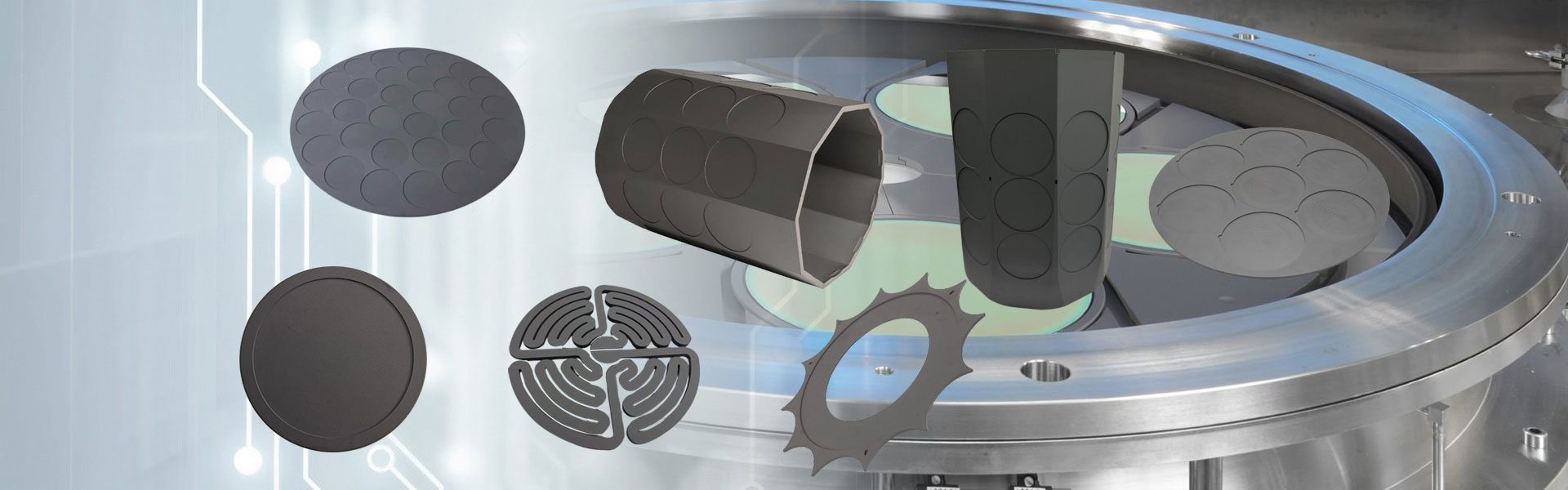
CVD SiC materials, due to their unique combination of excellent thermal, electrical, and chemical properties, are well-suited for applications in the semiconductor industry, where high-performance materials are required. Chemical vapor deposited (CVD) silicon carbide (SiC) components are widely used in etching equipment, MOCVD equipment, Si and SiC epitaxy equipment, and rapid thermal processing equipment.
The largest market segment for CVD SiC components is etching equipment components. Due to its low reactivity to chlorine- and fluorine-containing etching gases and its electrical conductivity, CVD silicon carbide (SiC) is an ideal material for components such as focus rings in plasma etching equipment. CVD silicon carbide (SiC) components in etching equipment include focus rings, gas showerheads, trays, edge rings.
Take the focus ring, for example. This critical component is placed outside the wafer and in direct contact with it. Voltage is applied to the ring to focus the plasma passing through it, thereby focusing the plasma on the wafer and improving processing uniformity. Traditionally, focus rings are made of silicon or quartz. However, with the advancement of integrated circuit miniaturization, the demand for and importance of etching processes in integrated circuit manufacturing continues to increase. The power and energy of the plasma used for etching are also increasing, especially in capacitively coupled plasma (CCP) etching equipment, which requires even higher plasma energies. Consequently, focus rings made of silicon carbide are becoming increasingly popular.
Due to the high performance of CVD SiC and its ability to be sliced into very thin sections, it can also benefit sputter targets and all types of electrodes.
Process of Chemical Vapor Deposition (CVD)
CVD is a process that transforms a material from a gas phase to a solid phase, used to form a thin film or coating on a substrate surface. The following are the basic steps in CVD:
1. Substrate Preparation
Choose an appropriate substrate material and perform the appropriate cleaning and surface treating to produce a clean, flat surface with good adhesion.
2. Reactive Gas Preparation
Prepare the necessary amount of reactive gas or vapor and inject it into the deposition chamber by some means (gas supply system). The reactive gas can be an organic compound, a metal-organic precursor, inert gas, or other gaseous species.
3. Deposition Reaction
If all instrumentation is setup correctly the CVD process will begin under the pre-defined reaction conditions. The reactive gas that has been injected into the chamber will undergo some chemical or physical reaction on the substrate surface to form a deposit onto the substrate surface. The deposit formation can be the result of several types of processes depending on the deposition method, these include vapor-phase thermal decomposition, chemical reaction, sputtering, epitaxial growth, etc.
4. Control and Monitoring
At the same time during the deposition process, certain deposition parameters need to be controlled and monitored in real time if the observer wishes to ensure the best possible properties in the film are maintained. These include relevant temperature measurement, pressure monitoring, and regulation of gas flow, all the while aiming to keep the desired reaction conditions stable and constant.
5. Deposition Completion and Post-Processing
When either the deposition time, predetermined thickness, or method selected, is achieved the introduction of the reaction gas can be ceased and deposition process ended. Following the deposition, several pertinent post-processing methods (annealing, structural modifications, surface treatment, etc.) should be performed to improve the film performance/quality.
It's important to note that the specific vapor deposition process can vary depending on the deposition technology, material type, and application requirements. However, the basic process outlined above covers most common vapor deposition steps.


- View as

Cincin Pembumian Elektrod Atas
Cincin Pembumian Elektrod Atas Semicorex ialah komponen kawalan plasma CVD SiC ketulenan ultra tinggi yang menstabilkan potensi elektrik dan menyokong pengedaran plasma seragam dalam sistem etsa dan pemendapan semikonduktor termaju. Semicorex membekalkan gelang pembumian CVD SiC ketepatan dan komponen semikonduktor menghadap plasma di seluruh dunia, menawarkan dimensi tersuai, sifat elektrik dan penghantaran global yang boleh dipercayai untuk pengeluar peralatan semikonduktor terkemuka.*
Baca LagiHantar Pertanyaan
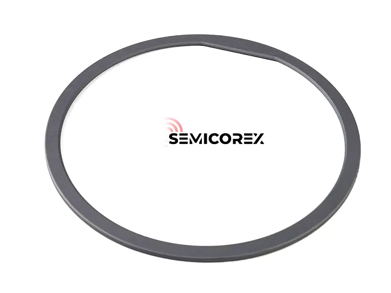
Mengukir Cincin Tepi
Semicorex Etching Edge Ring ialah komponen menghadap plasma CVD SiC ketulenan tinggi yang mengawal pengedaran plasma di sekeliling pinggir wafer, meningkatkan keseragaman goresan, ketepatan proses dan prestasi pembuatan semikonduktor keseluruhan. Semicorex menyediakan gelang fokus CVD SiC termaju, gelang pembumian, kepala pancuran mandian dan komponen kawalan plasma tersuai kepada pengeluar semikonduktor di seluruh dunia, disokong oleh kejuruteraan ketepatan dan bekalan global yang boleh dipercayai.*
Baca LagiHantar Pertanyaan
Sirip SiC CVD
Semicorex CVD SiC Fin ialah komponen silikon karbida pepejal berketumpatan tinggi yang tebal yang dihasilkan oleh Chemical Vapor Deposition, direka untuk aplikasi semikonduktor yang menghadap plasma dan suhu ultra tinggi yang memerlukan ketulenan, ketahanan dan rintangan kakisan yang luar biasa. Semicorex membekalkan komponen karbida silikon CVD termaju kepada pengeluar peralatan semikonduktor di seluruh dunia, menyediakan penyelesaian tersuai, kejuruteraan ketepatan dan penghantaran global yang boleh dipercayai untuk persekitaran proses yang paling mencabar.*
Baca LagiHantar Pertanyaan
Gelang Fokus Seramik untuk Semikonduktor
Cincin fokus seramik semicorex untuk semikonduktor ialah bahagian cincin berprestasi tinggi yang diperbuat daripada bahan CVD SiC, yang direka khusus untuk persekitaran etsa plasma berintensiti tinggi. Semicorex ialah pengeluar terkemuka industri cincin fokus seramik CVD SiC untuk semikonduktor, kami menantikan pertanyaan anda.
Baca LagiHantar Pertanyaan
Cincin Fokus SiC CVD Untuk 2L10-506419-21
Diperbuat daripada bahan CVD SiC berprestasi tinggi, cincin fokus Semicorex CVD SiC untuk 2L10-506419-21 ialah bahagian cincin penting yang disengineer khas untuk peralatan TEL VIGUS RK4 yang digunakan dalam proses goresan semikonduktor ketepatan. Memilih Semicorex bermakna anda akan memperoleh penyelesaian SiC CVD yang ideal untuk mencapai hasil goresan yang tepat dan seragam.
Baca LagiHantar Pertanyaan
Sirip Silikon Karbida Pepejal
Sirip karbida silikon pepejal semicorex ialah ketepatan komponen berprestasi tinggi yang dimesin daripada pepejal CVD SiC, yang digunakan terutamanya dalam relau suhu tinggi dalam peralatan rawatan haba semikonduktor. Semicorex komited untuk menawarkan sirip silikon karbida pepejal kejuruteraan tersuai dengan kualiti terkemuka pasaran untuk pelanggan kami yang dihargai, dan berharap untuk menjadi rakan kongsi jangka panjang anda di China.
Baca LagiHantar Pertanyaan
Semicorex telah mengeluarkan Cvd sic selama bertahun-tahun dan merupakan salah satu pengeluar dan Pembekal profesional Cvd sic di China. Sebaik sahaja anda membeli produk kami yang canggih dan tahan lama yang membekalkan pembungkusan pukal, kami menjamin kuantiti yang banyak dalam penghantaran cepat. Selama bertahun-tahun, kami telah menyediakan pelanggan dengan perkhidmatan tersuai. Pelanggan berpuas hati dengan produk kami dan perkhidmatan yang sangat baik. Kami amat berharap untuk menjadi rakan kongsi perniagaan jangka panjang anda yang boleh dipercayai! Selamat datang untuk membeli produk dari kilang kami.